← Don't Let Electrical Gremlins Stop Your 2002 Chevy Avalanche - This Wiring Diagram is Your Fix Electrical gremlins Schemas Echo avec PT2399: Les Secrets du Circuit Révélés Tape echo schematic at raymond eudy blog →
If you are looking for PCB Design Software for Printed Circuit Boards | Autodesk MY: Simplify you've came to the right page. We have 25 Images about PCB Design Software for Printed Circuit Boards | Autodesk MY: Simplify like How to Use a Modular Approach to Simplify Your PCB Design Process, Pads Viewer Free: Simplify Your PCB Design Review Process! Pads viewer and also Design for Better Signal Integrity by Rick Hartley | Sierra Circuits. Here it is:
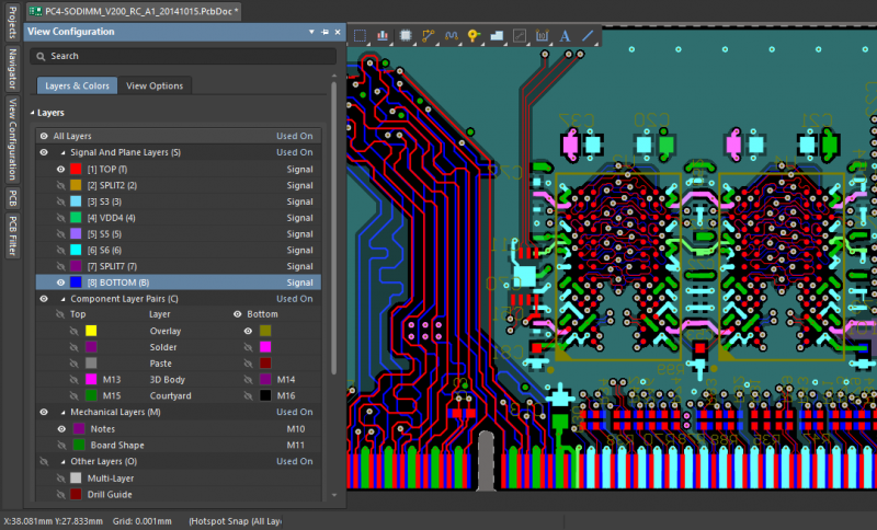
PCB Design Software For Printed Circuit Boards | Autodesk MY: Simplify
 diycircuit1.blogspot.com
PCB Design Software for Printed Circuit Boards | Autodesk MY: Simplify ...
GSM PCB Antenna: The Ultimate Networking Solution – PCB HERO
 www.pcb-hero.com
GSM PCB Antenna: The Ultimate Networking Solution – PCB HERO
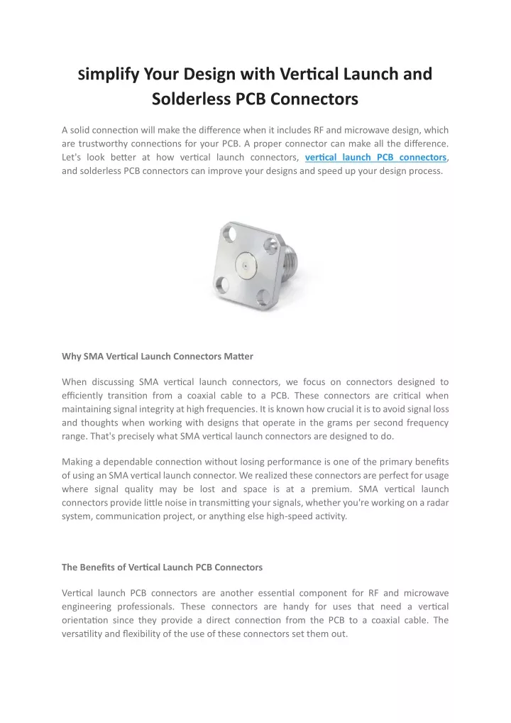
PPT - Simplify Your Design With Vertical Launch And Solderless PCB
 www.slideserve.com
PPT - Simplify Your Design with Vertical Launch and Solderless PCB ...
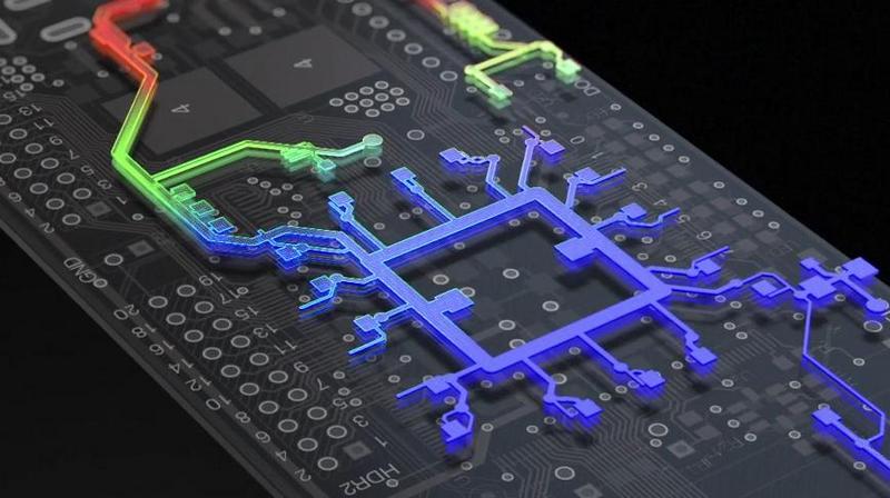
3D PCB Design Software Lets You Sculpt Your Design In Real Time - Altium
 www.altium.com
3D PCB Design Software Lets You Sculpt Your Design in Real Time - Altium
What Is Zero PCB Board? - MorePCB
 morepcb.com
What is Zero PCB Board? - MorePCB
EasyEDA Tutorial
 docs.easyeda.com
EasyEDA Tutorial
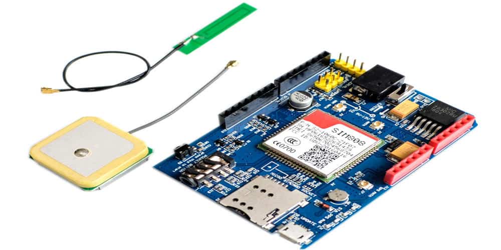
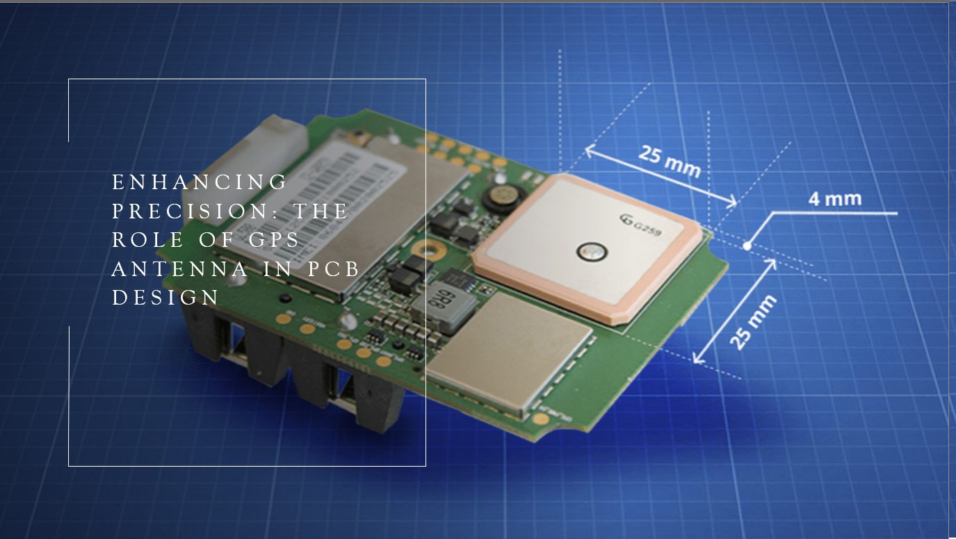
Importance, Design & Function Of GPS PCB Board
 hillmancurtis.com
Importance, Design & Function of GPS PCB Board
How To Use A Modular Approach To Simplify Your PCB Design Process
 www.linkedin.com
How to Use a Modular Approach to Simplify Your PCB Design Process
Mastering The Art Of PCB Design Basics | Sierra Circuits
 www.protoexpress.com
Mastering the Art of PCB Design Basics | Sierra Circuits
Pads Viewer Free: Simplify Your PCB Design Review Process! Pads Viewer
 wiringmistakes.blogspot.com
Pads Viewer Free: Simplify Your PCB Design Review Process! Pads viewer ...
Understanding Industrial PCB Production
Understanding Industrial PCB Production
2.4GHz PIFA - Saturn PCB
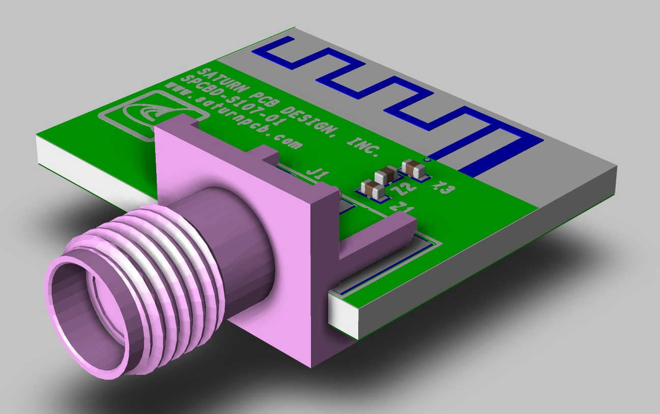 saturnpcb.com
2.4GHz PIFA - Saturn PCB
Choosing The Right PCB Etchback Process For Your Design
 hilelectronic.com
Choosing the Right PCB Etchback Process for Your Design
Raspberry Pi Printed Circuit Board (PCB) Diagram: Build Your Own IoT
 diywiringtips.blogspot.com
Raspberry Pi Printed Circuit Board (PCB) Diagram: Build Your Own IoT ...
EMI PCB Design: A Journey Of EMI Reduction And Discovery – Hillman
 hillmancurtis.com
EMI PCB Design: A Journey of EMI Reduction and Discovery – Hillman ...
How To Design For Pcb Manufacturing Sierra Circuits – Confopay
 confopay.com
How To Design For Pcb Manufacturing Sierra Circuits – Confopay
An Overview Of The Embedded PCB | Printed Circuit Board Manufacturing
 www.raypcb.com
An Overview of the Embedded PCB | Printed Circuit Board Manufacturing ...
Design For Better Signal Integrity By Rick Hartley | Sierra Circuits
 www.protoexpress.com
Design for Better Signal Integrity by Rick Hartley | Sierra Circuits
How To Design And Simulate PCB Antenna
 www.fedevel.com
How to Design and Simulate PCB Antenna
What Determines The PCB Cost? How To Reduce It? - MOKO
 www.mokotechnology.com
What Determines the PCB Cost? How to Reduce It? - MOKO
The Best PCB Antenna Design Software Eases Antenna Implementation
 resources.altium.com
The Best PCB Antenna Design Software Eases Antenna Implementation
Pads Viewer Free: Simplify Your PCB Design Review Process! Pads Viewer
 wiringmistakes.blogspot.com
Pads Viewer Free: Simplify Your PCB Design Review Process! Pads viewer ...
Gps Pcb Antenna Design At Kaitlyn Maund Blog
 storage.googleapis.com
Gps Pcb Antenna Design at Kaitlyn Maund blog
PCB Design Engineer Resume Sample (2023)
 itchol.com
PCB Design Engineer Resume Sample (2023)
Pcb Printers - Egpsawe
 egpsawe.weebly.com
Pcb printers - egpsawe
Gps pcb antenna design at kaitlyn maund blog. Pcb design engineer resume sample (2023). An overview of the embedded pcb